Search This Blog

Saturday, April 13, 2013

Educational Game

EDUCATIONAL BOARD GAME PROJECT


Educational Game


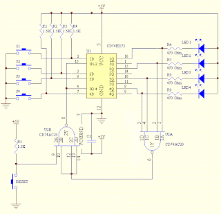
This educational game project can be used in a quiz competition to see which of the participants press the button first to answer questions posed by the quiz master. This constructional project is based on a latch CD74HC75 IC and a 4 input CD74AC20 NAND IC. The first person to press the switch will light up the LED designated for the person. The rest of the LEDs will not be able to be activated until the RESET button is pressed.


The truth table of the Latch IC and the NAND IC is as shown in the figures below.


Schematic Diagram


Initially when RESET button is pressed, the output of NAND gate from U2A will be logic "0" as all the inputs are at logic "1"state. As shown in the truth table for NAND gate, when all the inputs are "1", its output will be "0". Hence the output of NAND gate from U2B will be logic "1" since an input of "0" will cause it to go to logic "1". The logic "1" to the latch indicates that it is ready to output any data once any of the button is pushed.
If the first button pushed is S1, the logic at its output 1Q will be logic "0" and caused LED1 to light up. At the same time,it caused the output of U2A to go into logic "1". Hence the output of U2B will be logic "0" causing the latch to be disable which means that the outputs of all the latches will be at their previous state. As a result, the player who pressed button S1 will be shown as the one who is first to press the button and so qualify to answer the question.
The RESET button will be pressed by the quiz master to prepare the circuit for the next game.

Parts List


Time Delay Circuit


Time Delay Circuit


Looking for a simple time delay circuit? In the design of analog circuits, there are times when you would need to delay a pulse that came into a circuit before being used for the next process. This circuit uses a 555 timer to delay a pulse that comes in to a maximum time of 75 seconds. The timing of the delay can also be changed by changing the resistor value of VR1 and the capacitor value of E based on the time delay formula of t=0.69RC.


In order for the output to go high, the reset pin of 555 timer (pin 4) must be high and the TRIGGER pin (pin 2) voltage level must be below a third of the level of the power supply to the IC. When there is no pulse being applied to the input, transistor Q1 will turn ON and capacitor E is charged.


Once a pulse is applied to the input, transistor Q1 will turn OFF and pin 4 reset pin is held to high. This caused the capacitor E1 to be discharged through VR1 resistor. The time delay will depend on the discharged of capacitor E to a third of the supply before the output of 555 goes high. Experiment with different values of VR1 and E to get different time delay.
If the maximum value of potentiometer is set to 5M ohm, the time delay of the pulse will be 75 seconds.

Parts List


This is a good project to embark on if you are a beginners to electronic design. There are only 5 components needed to construct this circuit. It will provide you a good hands-on experience of using the 555 integrated circuit, one of the most commonly available IC widely in use for the past decades.


Police Siren Project

POLICE SIREN CIRCUIT DIAGRAM
POLICE SIREN MINI PROJECT
POLICE SIREN 555


Police Siren Project


This police siren simulated electronic project uses two 555 timers IC to generate a sound similar to the police siren. A single 556 timer IC which consists of two 555 timers can also be used. In this circuit, both of the timers are configured as astable circuit.
The first timer is configured as a square wave close to 1 Hz astable oscillator. The output of this timer is used to feed the control voltage of the second timer where it is subjected to frequency modulation. This frequency modulation will generate a tone similar to the siren used by the police.


The frequency of this tone generator can be varied by changing the value of potentiometer VR1. When set to its maximum value of 220k ohm, it will have a tone frequency of approximately 320 Hz.

Schematic Diagram

When S1 is switched ON, the circuit will be powered ON and U1 will start to oscillate at a frequency given by the formula:
f = 1.44/[(R1 + 2R2)(E1)] 
= 1.44/[(10 + 2*82)(10)] Hz 
= 0.8 Hz 
This output frequency from pin 3 of U1 is fed into pin 5 of U2 where it is subjected to frequency modulation through resistor 10K. The tone generated can be varied by changing the values of potentiometer VR1.
Experiment with the sound and settle with the best sound of your choice. The output of U2 is used to drive a power transistor which in turn drives an 8 ohm speaker. Diode D2 is used to prevent the damage of transistor Q1 due to the back emf generated by the speaker during the ON/OFF driving of the speaker.
A good way to start is to assemble all the components on a breadboard and connecting all of them using jumper wires on the board. Power up the board using 9V DC power supply and test the functionality of the circuit before proceeding to solder them onto the PCB strip board.
If you want to go further, try drawing the schematic diagram followed by the layout of the PCB pattern, etch the board, drill, assemble and solder the parts before testing them.

Parts List


LED Light Flasher

LED LIGHT FLASHER PROJECT
LED LIGHT FLASHER CIRCUIT DIAGRAM
 LED LIGHT FLASHER MM74C04


LED Light Flasher


This is a simple LED light flasher project that uses a CMOS 74C04 Integrated Circuit to alternately ON and OFF two LEDs that are connected in parallel. The Hex inverter MM74C04 from Fairchild Semiconductor has a wide operating power supply voltage range from 3V to 15V DC. It has a typical low power consumption of 10nW/package and has high noise immunity.


It is back to back compatible with the standard 74 logic family which is freely available in the market. All its inputs have diode clamps to VCC and GND which protect them from damage due to electrostatic discharge.

Schematic Description

The schematic above shows the simple configuration of the project. It uses two inverters U1A and U1B to form an oscillator configuration where the frequency of the oscillation is given by:
f = 1/[1.4RC]
= 1/[1.4(10 M Ohm)(0.1uF)]
= 0.7 Hz
The square wave frequency of 0.7 Hz is used to feed the input of U1D which is used as a buffer circuit. At the same time, the other inverter U1C gets its input from pins 2 and 3 of U1. With this configuration, when U1D output is high, U1C output will be low and vice versa. In this way when LED1 is ON, LED2 will be OFF and this will alternate at a frequency of 0.7Hz.
The current that goes through the LED is given by:
I = (9V-7V)/510 ohm
= 14mA

It is assumed that the voltage drop across each diode is 2V when it turns ON. One can experiment with the oscillation frequency by changing the values of R1, R2, R3, and C1. The brightness of the LEDs can also be changed by changing the values of the resistor R4. However, always ensure that the current through the LEDs is not exceeded or else the LEDs will be damaged.

Parts List


Electronic Timer Switch

ELECTONIC TIMER SWITCH PROJECT
ELECTONIC TIMER SWITCH CIRCUIT


Electronic Timer Switch


This electronic timer switch project is a good project to build to simulate the presence of occupants in a house. In these days when security is becoming more of a concern when no one is at home, having this device will deter the thief from breaking in.


When power up, after 60 minutes, the relay will turn ON for 100 secs, OFF for the next 100 secs, and ON again for 100 secs before OFF again for the next 60 mins. This sequence will be repeated. A device such as a lamp that is connected to the relay will turn ON and OFF according to this timing.

Schematic Diagram
The schematic of the project is as shown below.

The core of this electronic timer switch project uses a CD4060B binary counter. The binary counter has 10 outputs and the counter are counted by configuring the oscillator. Every negative clock will trigger the counter of the IC internally.
The timing of the circuit is affected by resistor R3(1M ohm) and capacitor C2(0.1uF). By connecting the four outputs in an AND configuration, the transistor Q1 will only turn ON if all the 4 outputs are in logic "1". If any of the logic is "0", the transistor will remain OFF.
For a complete cycle, the transistor will be ON twice when the output at pin 15, QJ goes to logic "1" and "0" twice when the other outputs QL, QM and QN remain at "1". When this happen, the relay K1 will switch status accordingly. The timing of the switching can be changed by changing the resistor values R2, R3 and C2. Download the data sheet of CD4060B from Texas Instruments for more details.
Note that since the oscillator is not using crystal, the timing may not be as accurate compared to the ideal calculation. In most cases, fine tuning the resistor and capacitor are good enough to make this project a success. To check whether the circuit is working, connect a LED in series with a 390 ohm resistor at output QD. It will flash ON and OFF as the oscillator oscillates.


Best Product On Amazon Must Buy

Best Electronics Soldering Iron Kit - https://amzn.to/3gIulii

Best Desoldering Pump Soldering Iron - https://amzn.to/3egN4Qp

Best Screw Driver Set For Repairing - https://amzn.to/2OsA0ND

Best Cord less Screw Driver Set - https://amzn.to/3eqvtWw

Best & Cheap Digital Multimeter - https://amzn.to/467dOOb

Best Fold Scope Microscope Basic Kit - https://amzn.to/393WI6o

Best & Smallest 60x Microscope - https://amzn.to/477r5HQ

Microware-20x-to-1000x-8 Led-usb -   https://amzn.to/2W8DGs0

Best Magnifying-Soldering-Stand - https://amzn.to/2ZVcZrM

Supper LED TV Backlight tester - https://amzn.to/3gLyXEo

Mini Hand Drill and 20pcs Drill Bits - https://amzn.to/3fiEWAc

Popular Posts